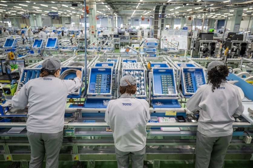
Japan's TOTO Ltd. — one of the world's most recognized makers of luxury bathroom fixtures — confirmed this week that its semiconductor ceramics business has become the dominant profit engine of the company, and that capital spending on chip-related products will soon outpace investment in the toilet and bathroom hardware that has defined the brand for a century. CTO Ryosuke Hayashi made the disclosure in an interview carried by Bloomberg and Business Standard on June 3, 2026.
With the company's large-scale expansion plans in the United States and China for housing equipment now complete, Hayashi said the ratio of spending on its plumbing-fixtures operations versus its semiconductor components operations will invert. Shares of TOTO jumped 11% in Tokyo on June 3 — their biggest single-day gain in more than a month — on the news. That move followed an 18% surge on May 2, when TOTO disclosed that its advanced ceramics division generated ¥28.9 billion (approximately $182 million) in operating profit for the fiscal year ended March 31, 2026, surpassing the profit from its core housing-equipment business and accounting for more than half of the company's record ¥53.8 billion in group-wide operating profit.
TOTO Ceramics Division: Semiconductors Displace Bathrooms as Profit Source
The inversion represents a structural shift more than a decade in the making. TOTO's advanced ceramics division was established in 1984 and began mass production of electrostatic chucks — precision ceramic components used in semiconductor manufacturing equipment — in 1988. For roughly three decades the business operated at a loss or barely broke even. What changed was the AI infrastructure buildout: as data center operators poured capital into artificial intelligence workloads, demand for NAND flash memory accelerated, NAND manufacturers raced to expand production capacity, and demand for the specialized components inside their manufacturing equipment surged accordingly. TOTO's ceramics division now carries an operating margin of approximately 43% — compared to roughly 4% for the housing equipment segment that makes up about 91% of the company's revenue.
The company is allocating approximately ¥30 billion (about $190 million) toward semiconductor-related capital expenditure and research through fiscal year 2028. A new kiln building is under construction at TOTO's plant in Buzen, Fukuoka Prefecture — groundbreaking took place in December 2025 — and is scheduled for completion in January 2027, at which point the company's electrostatic chuck production capacity will exceed current levels by more than 20%, according to Hayashi.
Read more: Samsung Electro-Mechanics AI Server Pivot: R&D Surges 36%, Capacity Cannot Match Big-Tech Demand
How TOTO Electrostatic Chucks Work: Cryogenic Etching and 3D NAND Demand
An electrostatic chuck is a disc, roughly the diameter of a steering wheel, that holds a silicon wafer flat and motionless during chip fabrication processes. Where a mechanical clamp would scratch the wafer's surface and a vacuum-based chuck requires ambient pressure conditions incompatible with the plasma environments inside modern fab tools, electrostatic chucks use a voltage applied across embedded electrodes in a sintered ceramic body to generate an electrostatic field — the Coulomb force or its temperature-dependent variant, the Johnsen-Rahbek force — that pins the wafer without physical contact.
TOTO's specific competitive advantage is concentrated in one of the most demanding applications in modern chip manufacturing: cryogenic dielectric etching for 3D NAND flash memory. Building 3D NAND — the type of flash memory inside AI data center storage drives — requires drilling extremely narrow, deep holes through hundreds of vertically stacked memory cell layers. As of 2026, leading 3D NAND architectures stack more than 200 such layers, and industry roadmaps project reaching 1,000 layers by the end of 2030. Each of those holes must be etched with an aspect ratio exceeding 50:1 — more than 50 times deeper than the hole is wide — at tolerances measured in nanometers.
Conventional reactive ion etching fails at these depths because the chemical reaction rate drops off as the etchant penetrates deeper into a narrow channel, producing bowed walls and incomplete profiles. Lam Research, the dominant supplier of etching equipment to NAND manufacturers, developed its Lam Cryo cryogenic etch platform to address this. By chilling the wafer surface to below -100°C using liquid nitrogen-cooled channels within the electrostatic chuck, cryogenic etching changes the etch chemistry in ways that suppress unwanted sidewall reactions while maintaining the ion bombardment needed to drive the process vertically. Lam Cryo 3.0, the current generation introduced in July 2024, etches memory channels more than 50 times deeper than their width with a profile deviation of less than 0.1%.
TOTO is a primary supplier of electrostatic chucks for Lam Research's cryogenic etch tools. Analysis by UK Investor Magazine positions TOTO as the global second-largest electrostatic chuck producer, noting that TOTO and Lam Research have co-developed chamber-level components since 1990 and that Lam awarded TOTO its Supplier Excellence Award in both 2023 and 2024. The NAND manufacturers operating those Lam Research tools — and therefore driving replacement and new-unit demand for TOTO's chucks — include Samsung, SK Hynix, Micron, and Kioxia.
Why Toilet Ceramic Expertise Transfers to Chip Manufacturing
The chemistry connecting TOTO's plumbing heritage to its semiconductor role is alumina — aluminum oxide, Al₂O₃ — the dominant material in both high-end ceramic sanitary ware and precision electrostatic chucks. The challenge in both applications is not obtaining alumina but firing it with the microstructural uniformity that demanding performance requirements demand.
TOTO's proprietary alumina formulations combine alumina at purities of 99.4% or higher with precisely controlled additions of titanium dioxide, tuning the ceramic's electrical volume resistivity to the narrow 10⁸ to 10¹¹ ohm-centimeter range that allows the electrostatic clamping mechanism to function correctly across the full range of semiconductor process temperatures. The ceramic must also remain dimensionally stable under repeated cycling between the extreme cold of cryogenic etching and the plasma-generating conditions of other process steps. Grain size is controlled to an average particle diameter of 2 micrometers or less to minimize surface roughness after plasma exposure — because particles dislodged from a degraded chuck surface fall onto the wafer and destroy the circuit being fabricated.
It is the sintering and kiln-firing methodology — the same process engineering that TOTO spent decades refining to produce vitreous china toilet bowls with dimensional tolerances tight enough for precision-fit plumbing components — that gives the company its materials advantage in chucks. Competitors can produce alumina components; what they cannot easily replicate is TOTO's accumulated process knowledge about how to fire complex ceramic geometries at scale while maintaining the purity, grain uniformity, and dimensional accuracy that high-performance semiconductor applications require.
TOTO Expanding Beyond NAND: Aerosol Deposition and Chiplet Integration
TOTO's ceramics ambitions extend beyond electrostatic chucks for memory manufacturing. The company produces a second family of products using aerosol deposition (AD) technology — a process in which ceramic powder is accelerated in a gas jet and deposited at room temperature onto chamber walls inside etching tools for logic-chip manufacturing, forming a dense protective coating that resists plasma erosion. Unlike sintered ceramics, AD coatings can be applied to complex three-dimensional geometries and are already in use in advanced logic-chip fab lines. TOTO's three product lines — electrostatic chucks for NAND etching tools, aerosol deposition components for logic-chip chamber walls, and structural parts for display manufacturing equipment — reflect a deliberate effort to diversify its semiconductor revenue base.
The company is also pursuing a position in chiplet integration — the architecture in which multiple chips are interconnected in a single package to achieve performance that a monolithic die cannot. According to reporting by Nikkei, TOTO sees its ceramic structural components as a strong fit for chiplet fixture materials, with development work already underway. If chiplet-based packaging becomes the standard form factor for AI accelerators and advanced processors — as current industry roadmaps suggest — the surface area of opportunity for precision ceramic components extends well beyond NAND etching.
Activist Campaign Credited With Driving Investor Attention
TOTO's re-rating by investors did not happen without external pressure. In February 2026, UK-based activist fund Palliser Capital — which had taken a position among TOTO's top 20 shareholders — published a detailed value enhancement plan arguing that the market was severely undervaluing the ceramics business because the company provided inadequate disclosure about it. Palliser called TOTO "the most undervalued and overlooked AI memory beneficiary," estimated the company's ceramics segment held a five-year competitive lead over rivals, and projected more than 55% upside in the stock if TOTO improved its communications and capital allocation. Goldman Sachs had upgraded TOTO to Buy earlier that month. The combination of the Goldman upgrade, the Palliser campaign, and the subsequent record earnings disclosure produced the back-to-back share surges in May and June.
The risk scenario is familiar to anyone who has tracked semiconductor components: NAND memory is cyclical, and an aggressive capacity expansion in chuck manufacturing could collide with a demand downturn if AI storage spending decelerates. Hayashi acknowledged on the record that ceramics margins are sensitive to equipment depreciation costs and currency movements, telling Bloomberg that "sales will definitely grow" but stopping short of guaranteeing margin stability. For investors and procurement professionals, that caveat is the relevant constraint — the structural demand driver is real, but so is the cyclicality of the underlying memory market.
Frequently Asked Questions
What does TOTO make for semiconductor manufacturing?
TOTO produces electrostatic chucks — precision ceramic discs that hold silicon wafers flat during etching, deposition, and other plasma-based fabrication processes — along with aerosol-deposition chamber components and structural parts for display manufacturing equipment. Its electrostatic chucks are used specifically in Lam Research's cryogenic etch tools, which carve the deep, narrow holes needed for advanced 3D NAND flash memory production.
How does an electrostatic chuck work in a semiconductor fab?
An electrostatic chuck uses voltage applied to embedded electrodes inside a sintered alumina ceramic body to generate an electrostatic field that pins a silicon wafer against its surface without mechanical contact. In cryogenic etching applications, the chuck also circulates liquid nitrogen to hold the wafer at temperatures below -100°C, allowing the etch chemistry to achieve the high aspect ratio profiles required for 3D NAND memory cell channels.
Why is TOTO stock rising because of AI demand?
TOTO's advanced ceramics division now generates more than half of the company's total operating profit — despite representing less than 10% of its revenue — because semiconductor ceramic components carry operating margins of roughly 43%, far above the roughly 4% margin of its toilet and bathroom fixture business. AI-driven data center expansion has accelerated NAND demand, sending both replacement orders and new-capacity orders to TOTO.
What is the Japan AI supply chain connection for semiconductor components?
Japan's industrial base includes a network of companies whose expertise in precision materials and manufacturing — originally developed for consumer and industrial applications — translates directly into critical semiconductor supply chain roles. TOTO is among the most prominent examples, alongside Ajinomoto (amino-acid chemistry used in chip insulating films) and Kao (wafer cleaning agents derived from cosmetics expertise). This heritage gives Japanese suppliers structural process know-how advantages that take years for competitors to replicate.
ⓒ 2026 TECHTIMES.com All rights reserved. Do not reproduce without permission.


