Nvidia plans to introduce an architecture in its upcoming Vera Rubin platform that lets GPUs issue storage commands without going through the CPU at all — a shift that a prominent semiconductor researcher says could set the stage for a new class of flash memory offering more than sixteen times the capacity of today's high-bandwidth memory stacks. Song Ki-hwan, a professor in the Department of System Semiconductor Engineering at Yonsei University, revealed the plans on May 18 at the 2nd Semiconductor Device Frontier Summit in Seoul, making this one of the first public characterizations of Nvidia's storage strategy for the Vera Rubin generation.
What GIDS Does That GPU Direct Storage Does Not
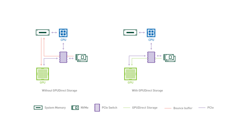
Nvidia's existing GPU Direct Storage architecture already shortens the data path by letting storage stream data straight to the GPU, bypassing system DRAM. But the CPU still initiates every request. GPU-Initiated Direct Storage Access, or GIDS, removes the CPU from the loop entirely: the GPU itself issues the read command to storage, retrieves the data, and manages the transfer — no CPU thread required.
"GIDS is one step beyond GPU Direct Storage," Song said. "The GPU fetches data straight from storage, and Nvidia has opened up a new market with it."
Microsoft and AMD are also evaluating similar GPU-driven storage approaches, Song noted, suggesting the architecture is becoming a focal point for the industry rather than a proprietary Nvidia decision.
The case for eliminating CPU mediation is structural. In a conventional von Neumann computing setup, a CPU receives a storage request, retrieves data into DRAM, then hands it to the GPU — two hops that consume time and power at every step. CPUs are fundamentally limited in the number of threads they can manage simultaneously, making them a bottleneck when feeding the parallel appetite of modern AI accelerators. A GPU, by contrast, can dispatch tens of thousands of concurrent operations at once, making it far better suited to drive high-throughput storage input and output directly.
Why GIDS Requires a Better Class of Flash
Elevating the GPU to storage controller raises the bar for the underlying NAND flash. Storage now has to respond at GPU speeds and at GPU scale, which conventional solid-state drives — even fast NVMe drives — are not designed to do. That gap is precisely where High Bandwidth Flash, or HBF, enters the picture.
HBF applies the same vertical-stacking principle that made High Bandwidth Memory possible. Multiple NAND flash dies are stacked and interconnected with through-silicon vias, or TSVs, dramatically increasing the bandwidth and density a single package can deliver. Sandisk, which pioneered the concept, is targeting a 16-die-plus-base-die flash stack that fits the same physical footprint as an HBM package, delivering read bandwidths of 1.6 terabytes per second and capacities up to 512 gigabytes per stack — versus the approximately 64 gigabytes per stack that HBM4 currently offers.
The density advantage of NAND over DRAM is the key lever. NAND offers approximately thirty times the bit density of DRAM per unit area. That ratio means a GPU package combining six HBF stacks with two HBM stacks could carry around 3,120 gigabytes of total memory — compared with 192 gigabytes for an eight-stack HBM-only configuration today. The practical implication, Song noted, is the ability to run AI models with roughly sixteen times more parameters on a single package.
"Although HBF is not yet a mainstream industry technology, I believe it can solve the technological challenges of the agentic AI era," Song said. "If we look past the device level to the full system and market, and take on new technologies, we can lead a paradigm shift."
The Hard Constraint: HBF Cannot Replace HBM
The capacity gains come with a firm boundary. NAND flash tolerates only around 100,000 program-and-erase cycles before it degrades — a tiny fraction of DRAM's effectively unlimited write endurance. That write limitation makes HBF unsuitable for any workload that writes frequently.
The most important example is the key-value cache, or KV cache, which is the running memory an AI model continuously writes and rewrites during inference as it processes each new token in sequence. The KV cache cannot move to HBF. Most of the speed lost in flash occurs in the write cycle — a constraint intrinsic to how NAND stores charge — while flash's read performance can in principle match or exceed DRAM.
What HBF can store are model parameters — the trained weights that define an AI model's behavior. Parameters are written once during training and remain effectively read-only during inference, imposing almost no wear on the NAND. They are also, by far, the largest component of what an AI system needs to hold: a large language model's parameter set dwarfs its KV cache in size by orders of magnitude. Storing parameters in HBF while keeping the KV cache in HBM is the hybrid architecture that Song and industry analysts see as the natural operating mode for next-generation AI accelerators.
Steven Woo, a fellow and distinguished inventor at Rambus, has described HBF as "gaining attention as system designers look for new memory tiers that sit between DRAM and traditional NAND." Xi-Wei Lin, executive director of applications engineering at Synopsys, noted that the technology was designed specifically to store all AI model parameters next to the GPU, eliminating the need for them to leave the package.
Power Costs and the Case Against More HBM Stacks
The pressure to find an alternative to HBM-only configurations is not just about capacity. Song cited estimates suggesting that roughly half of total system power in current AI servers is consumed moving data between physically separated GPUs and HBM stacks. Adding more HBM layers does not resolve the physics — the data still has to travel between packages. Placing dense, fast flash directly within the GPU package shortens that trip fundamentally, with the potential to reduce the energy cost of data movement even as model sizes keep expanding.
Sandisk, SK Hynix, and the Standardization Race
Sandisk and SK Hynix formalized a standardization effort for HBF in February 2026, establishing a dedicated workstream under the Open Compute Project to define universal specifications. Samsung has also joined the effort. Sandisk is targeting first HBF memory samples in the second half of 2026, with the first AI inference devices built around HBF expected to sample in early 2027. Alper Ilkbahar, Sandisk's chief technology officer, said the collaboration is "setting the bar for the next era of AI computing."
Wiwynn, a server manufacturer, showcased Nvidia's Storage-Next initiative at GTC 2026 in March, describing a GPU-initiated storage architecture that orchestrates input and output directly across a 96-drive NVMe array via the GPU — an early commercial signal that the GIDS concept is already being built into rack-scale infrastructure.
Vera Rubin itself — the platform Song identified as GIDS's first deployment — is in full production, with availability from partners targeted for the second half of 2026, according to a Nvidia press release from January 2026. Among the first cloud providers to deploy Vera Rubin-based instances are AWS, Google Cloud, Microsoft, and Oracle Cloud Infrastructure.
The convergence of these timelines means the GIDS architecture and its enabling flash memory tier are not a distant roadmap item. They are arriving together, in the same product cycle, with the standardization infrastructure to support them already under construction. Whether that combination delivers on the 16× capacity promise will depend on how well the AI software stack adapts to the read-heavy, write-cautious regime that HBF demands.
ⓒ 2026 TECHTIMES.com All rights reserved. Do not reproduce without permission.


