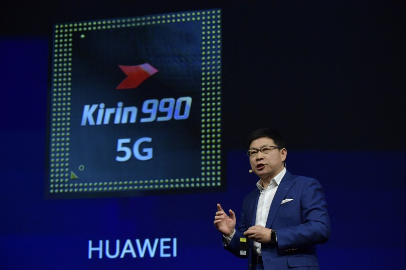
Huawei unveiled a new chip-design framework called the Tau Scaling Law at the 2026 IEEE International Symposium on Circuits and Systems in Shanghai on May 25, proposing to replace Moore's Law with a metric focused on signal-travel time — and claiming a 53.5% transistor density increase for its upcoming Kirin 2026 processor. Not a single independent auditor has verified those numbers.
He Tingbo, president of Huawei's semiconductor division HiSilicon, delivered the keynote in a rare public appearance, announcing that the first commercial chip built on the framework — the Kirin 2026, which will power the Mate 90 smartphone series — arrives this autumn. The announcement triggered a 7.6% surge in shares of SMIC, Huawei's primary Chinese manufacturing partner.
The core claim is significant, if unproven: Huawei says its new LogicFolding architecture — which reorganizes chip circuits from flat two-dimensional grids into vertical three-dimensional stacks — delivers a 53.5% increase in transistor density (from 155 MTr/mm² to 238 MTr/mm²), a 41% improvement in performance-core energy efficiency, and a peak clock speed of 3.1 GHz, all without requiring any advanced lithography equipment China cannot currently access. Huawei says it has already designed and mass-produced 381 chips over the past six years using earlier iterations of the framework.
Read more: Huawei Will Develop Cutting-Edge Semiconductors, Chips by 2031 to Compete With Samsung, TSMC
What Is Huawei's Tau Scaling Law?
Moore's Law — the decades-old observation that transistor counts double roughly every two years through physical miniaturization — has run into severe physical limits and sharply rising costs, with advanced-node chip designs now exceeding $1 billion per project. Huawei's Tau framework proposes a different optimization target: rather than shrinking the space between transistors, engineers should minimize τ, the Greek-letter symbol for the time it takes signals to travel through every layer of a computing system.
The framework addresses the entire stack: transistor switching speed, local interconnect resistance, circuit-path lengths, chip-level architecture, memory access latency, packaging, and data-center communication. LogicFolding is the architectural expression of this principle, stacking layers of silicon vertically to shorten critical signal paths and reduce resistive and capacitive loads, achieving density gains without requiring a newer or more expensive process node. He Tingbo positioned the Tau Law not merely as Huawei's internal design philosophy but as a proposed industry-wide principle — the first such framework to originate from a Chinese company.
LogicFolding vs. TSMC: What the Density Numbers Actually Mean
The 53.5% density claim requires context. At 238 million transistors per square millimeter, the Kirin 2026 chip on SMIC's roughly 7nm-class node would sit approximately 40 million transistors per square millimeter short of TSMC's current 3nm process. Qualcomm's rumored Snapdragon 8 Elite Gen 6 Pro runs performance cores at a reported 5.0 GHz — nearly 2 GHz faster than the Kirin 2026's 3.1 GHz peak.
More significantly, all of these figures are first-party data. NBC News noted in its coverage of the keynote that Huawei "did not provide any independent performance data to support its announcement." Omdia analyst Lian Jye Su, quoted in Wall Street Journal reporting cited by SiliconAngle, offered a measured assessment: the Tau approach is "an alternative path forward, and a breakthrough Huawei managed to find while facing supply chain challenges" — while adding that "it remains to be seen if Huawei can really do this."
The 2031 target compounds the timeline gap. Huawei projects that chips built under the Tau framework will reach transistor density equivalent to a 1.4nm process by 2031, three years after TSMC plans to begin mass production of actual 1.4nm chips in 2028. Bloomberg and the Taipei Times separately confirmed the current manufacturing gap between TSMC and Huawei-plus-SMIC stands at roughly five years.
Sanctions Context: Architecture Built Around Restricted Equipment
The technical and geopolitical narratives are inseparable. Since 2019, Huawei has been barred from acquiring ASML's extreme ultraviolet lithography machines, the equipment Western foundries use to manufacture chips at 7nm and below through conventional geometric scaling. The US Commerce Department placed Huawei on its Entity List in May 2019; the FCC added it to its Covered List in June 2020, formally designating the company a national security threat.
The Tau Law is, by Huawei's own description, an architectural response to those restrictions. Rather than competing on a dimension that requires equipment China cannot obtain, Huawei has pivoted to a dimension — signal-latency optimization — where design tools and existing process nodes remain accessible. The approach is conceptually coherent: Samsung and TSMC both use 3D chip-stacking techniques, though for reasons driven by performance rather than sanctions compliance.
If the Kirin 2026 autumn launch produces independently verified density gains, it would increase pressure on US regulators to expand export controls on chip design tools. The Bureau of Industry and Security has already informed electronic design automation software suppliers they need a license for sales to China, per a September 2025 Congressional Research Service assessment.
Benchmark Claims Require Independent Verification
Analysts and independent media flagged a specific credibility gap in the ISCAS announcement: Huawei presented its performance figures without supplying a methodology for independent replication. Market Business News summarized the consensus position: Huawei "has not shown that it can produce 1.4nm-equivalent chips at scale, and has not shown that LogicFolding can match TSMC's most advanced processes on power efficiency, yield, or manufacturing reliability." One publication noted that at 238 MTr/mm², the Kirin 2026 chip "theoretically" approaches Intel 18A and TSMC 3nm density — but in semiconductor manufacturing, yield, defect rates, and power envelopes determine whether density claims survive production at scale.
Semiconductor analyst William Martin Keating of Semicon Alpha noted that Huawei's 2031 target of "1.4nm-equivalent" density arrives three years after TSMC's A14 node enters actual volume production. The word "equivalent" carries weight here: Huawei's claim describes transistor density achieved through architecture and integration, not operation of a 1.4nm lithography process. The performance, yield, and power-efficiency properties of a density-equivalent chip built on older lithography have not been established by any independent party.
China National Intelligence Law Applies to All Huawei Products
Any organization considering Huawei hardware — whether a smartphone, networking equipment, or an AI accelerator — operates under a fixed legal condition that Huawei's stated privacy policies cannot override: China's National Intelligence Law of 2017 requires all Chinese organizations and citizens to "support, assist and cooperate with the state intelligence work." Article 22 of China's Counter-Espionage Law of 2014 separately requires organizations to "truthfully provide" information during state security investigations and "must not refuse."
The FCC cited the National Intelligence Law by name in its June 2020 order formally designating Huawei a covered company under national security rules, finding that the law "compels [Huawei] to assist the Chinese government in espionage activities." Huawei has publicly denied that it provides or would provide user data to the Chinese government; that denial has never been tested in an independent court proceeding. No backdoor has been confirmed in the LogicFolding architecture specifically, but the legal obligation for cooperation with Chinese state intelligence exists regardless of the chip architecture in question.
Ecosystem and Operational Gaps for International Customers
For enterprises and developers outside China, adopting Huawei's Kirin-powered hardware or Ascend AI chips carries operational friction that benchmark figures do not capture. The Bureau of Industry and Security ruled in May 2025 that Huawei's Ascend 910B, 910C, and 910D AI chips are prohibited for all persons — US and non-US — to use, sell, export, or finance. International teams building or procuring Ascend-based infrastructure risk sanctions exposure. Huawei's road to Ascend-based AI data centers by 2030 depends on LogicFolding scaling into those processors, but enterprise customers outside China face a binary choice: comply with US restrictions and forgo the architecture, or risk sanctions liability.
Support, documentation, and tooling for the Tau-based ecosystem remain entirely first-party. No independent electronic design automation workflow verified to work with LogicFolding's vertical integration methodology was publicly available as of the announcement date. For teams evaluating the architecture from outside China, the path to production deployment is undefined.
Frequently Asked Questions
What is Huawei's Tau Scaling Law?
The Tau Scaling Law is Huawei's proposed replacement for Moore's Law as the guiding principle of semiconductor progress. Instead of measuring progress by how small transistors can be made, it measures progress by how much signal-travel delay — expressed as the time constant τ — can be compressed across every layer of a computing system, from individual transistors to data-center networks. Huawei presented the framework at IEEE ISCAS 2026 in Shanghai on May 25, 2026.
How does LogicFolding improve transistor density without EUV machines?
LogicFolding reorganizes traditional flat two-dimensional circuit layouts into vertical three-dimensional stacks, shortening critical signal paths and reducing the resistive and capacitive loads that slow chips down. By stacking silicon layers upward rather than shrinking transistors horizontally, Huawei claims it can achieve higher transistor density at the same process node — eliminating the need for ASML extreme ultraviolet lithography machines that US export controls have blocked from Chinese foundries. Huawei claims a 53.5% density increase for its Kirin 2026 chip compared to conventional designs, but no independent auditor has verified this figure.
Can Huawei match TSMC without access to leading-edge lithography?
Not yet, and possibly not by 2031. TSMC currently operates at a roughly five-year manufacturing lead over Huawei and SMIC. TSMC plans to begin mass production of true 1.4nm chips in 2028; Huawei targets a 1.4nm-equivalent transistor density by 2031 — three years later, and through architectural approximation rather than the same lithography process. The engineering principle behind LogicFolding is sound, but yield, power efficiency, and manufacturing reliability at scale remain unproven as of the Kirin 2026 announcement.
What does China's National Intelligence Law mean for Huawei hardware buyers?
China's National Intelligence Law of 2017 requires all Chinese organizations to cooperate with state intelligence work, an obligation that applies to Huawei regardless of which country its hardware is deployed in or what Huawei's own privacy policy states. The US Federal Communications Commission cited this law by name in its June 2020 order designating Huawei a national security threat and barring its equipment from US communications networks. International buyers of Huawei devices are making that purchase under a legal framework that requires the manufacturer's cooperation with Chinese state intelligence upon government request.
ⓒ 2026 TECHTIMES.com All rights reserved. Do not reproduce without permission.


