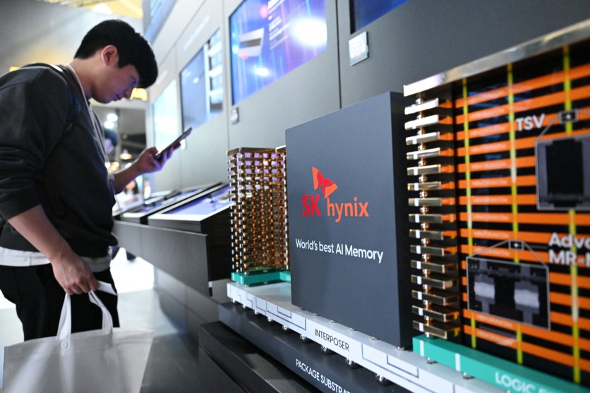
SK hynix, the South Korean chipmaker that supplies roughly 62 percent of all high-bandwidth memory sold globally, announced a new packaging architecture on May 26, 2026 that addresses one of the most persistent performance ceilings in AI data center hardware: heat buildup inside the HBM package itself. The technology, called iHBM (Integrated High Bandwidth Memory), embeds proprietary cooling elements directly within the memory package at the exact location where temperatures run highest, rather than relying on heat to escape through surrounding structures after it has already accumulated.
The announcement is timely. SK Group Chairman Choi Tae-won is scheduled to meet Nvidia CEO Jensen Huang at GTC Taipei 2026, held alongside Computex on June 1, where next-generation HBM requirements and the iHBM roadmap are expected to be central to the discussions.
High-bandwidth memory achieves its massive bandwidth advantage by stacking multiple DRAM dies vertically — today's top-end HBM products reach twelve layers — and placing them immediately adjacent to a GPU or AI processor on a silicon interposer. That proximity dramatically reduces the distance data must travel, but it also concentrates enormous amounts of heat into a very small area. The problem is not distributed evenly across the stack. It concentrates most intensely at the die-to-die physical layer, or D2D PHY — the high-speed electrical interface connecting the base of the HBM stack to the processor die beneath it. Switching activity, leakage effects, electrical resistance, and constant multi-terabyte-per-second data flow combine to make this layer a persistent thermal hotspot under sustained AI workloads.
When temperatures at the D2D PHY climb past safe operating limits, the system automatically throttles — reducing clock speeds and voltages to prevent physical damage. In an AI data center where accelerators run continuously under heavy load, those performance reductions translate directly into lower throughput, longer training runs, and higher operating costs.
How SK hynix HBM Cooling Works Inside the Chip
Conventional HBM designs rely on an indirect cooling path: heat generated deep inside the package travels through the core die and out through the package structure before it can be removed by an external cold plate. The core die acts as a thermal intermediary, and every layer of material it passes through adds resistance.
iHBM eliminates the detour. SK hynix places its Integrated Cooling Elements, or ICEs, directly inside the D2D PHY region — the very zone where heat concentration is highest — rather than waiting for heat to migrate away from its source. ICEs are made from a silicon-based material that does not conduct electricity but conducts heat exceptionally well, creating a dedicated thermal pathway within the package itself. The result, according to SK hynix, is a reduction in thermal resistance of more than 30 percent compared with conventional HBM designs, enabling stable operation even under sustained high-temperature and high-load conditions.
Choi Jae-hyuk, a professor at Seoul National University's Graduate School of Convergence Science and Technology, noted that the widened D2D PHY pathway created by modern HBM architecture leaves a specific structural space inside the package that iHBM exploits. The approach earned his assessment as "an excellent attempt" — using what he described as a "cooling pillar" to dissipate heat from a location where the space exists precisely because of the same design choices that created the thermal challenge.
HBM5 Packaging and Production Readiness
The commercial importance of iHBM extends beyond the thermal improvement itself. SK hynix built the architecture on its existing Advanced Mass Reflow Molded Underfill (MR-MUF) wafer-level packaging process — the same process platform that underpins its current-generation HBM products, which already feed Nvidia's AI accelerators at scale. That means iHBM can move into high-volume production without requiring new manufacturing equipment and without forcing customers to redesign their System-in-Package layouts.
Seoul Economic Daily reported that analysts specifically cited this characteristic as a competitive advantage in customer supply timelines: adoption requires minimal design changes on the buyer's side, which lowers the barrier for hyperscalers and AI chipmakers to specify iHBM as a requirement in their next-generation hardware. The same reporting notes that iHBM is designed to meet the thermal requirements of Nvidia's next-generation Rubin Ultra and Feynman accelerators, which are expected to operate at power densities reaching 230 kilowatts per rack.
SK hynix plans to introduce iHBM beginning with its HBM5 generation, which Counterpoint Research estimates will arrive around 2029 to 2030. HBM5 will push stack heights and data rates significantly beyond today's HBM4 products, and the thermal demands will increase accordingly.
Independent technical analyst Igor's Lab noted that while the 30 percent reduction in thermal resistance is meaningful, the figure will need to prove itself in real-world HBM5 systems before its full operational impact can be assessed. HBM5 production at scale remains several years out, leaving a gap between the announcement and customer validation.
Why AI Memory Overheating Caps the Next Scaling Cycle
The iHBM announcement reflects a broader shift in how the semiconductor industry is approaching performance gains. Adding more compute or stacking more memory layers no longer delivers proportional improvements when heat becomes the binding constraint. Research reported by TechRadar on Imec's work presented at the 2025 IEEE International Electron Devices Meeting demonstrated the severity of the problem in extreme configurations: a 3D HBM-on-GPU design reached peak GPU temperatures of 141.7°C without thermal mitigation, compared to 69.1°C for a conventional 2.5D configuration under the same cooling conditions. Halving the GPU clock rate brought temperatures below 100°C but reduced AI training throughput by 28 percent.
SK hynix holds approximately 62 percent of the global HBM market by shipment volume as of the second quarter of 2025, according to Counterpoint Research, supplying Nvidia, Google, Amazon, and other major AI infrastructure customers. At its first-quarter 2026 earnings call, the company stated that customer demand for HBM over the next three years already exceeds its production capacity. iHBM positions SK hynix to maintain that lead into the HBM5 generation by addressing the thermal barrier that would otherwise limit how far future products can scale.
Frequently Asked Questions
What is iHBM and how does it differ from regular HBM?
iHBM, or Integrated High Bandwidth Memory, is SK hynix's thermal packaging architecture that embeds silicon-based cooling elements directly inside the HBM package at the D2D PHY layer — the interface between the memory stack and the AI processor. Conventional HBM dissipates heat indirectly by routing it through the core die and outward; iHBM creates a dedicated heat path at the source, reducing thermal resistance by more than 30 percent.
Why does HBM memory overheat in AI accelerators?
HBM achieves high bandwidth by stacking multiple DRAM dies vertically and placing them directly adjacent to a GPU or AI processor. This arrangement concentrates heat in a very small area, particularly at the high-speed electrical interface connecting the memory stack to the processor. Under sustained AI workloads, heat buildup at this interface triggers automatic performance throttling — the system lowers clock speeds to prevent damage, directly reducing AI training and inference throughput.
What is HBM5 and when will it arrive?
HBM5 is the next generation of high-bandwidth memory after HBM4, targeting higher stack heights, faster data rates, and greater capacity for AI accelerators. Counterpoint Research estimates HBM5 will enter production around 2029 to 2030. SK hynix plans to incorporate iHBM into its HBM5 products, alongside the industry's expected shift to hybrid bonding — a method that connects stacked dies by joining copper directly without traditional bump structures.
How does iHBM affect AI data center cooling requirements?
By reducing in-package thermal resistance by more than 30 percent, iHBM allows AI accelerators to sustain higher performance levels for longer periods without triggering thermal throttling. For data center operators, this means more consistent throughput under the sustained heavy workloads characteristic of AI training runs. The technology is also compatible with existing System-in-Package designs, so customers can adopt it without rearchitecting their server cooling infrastructure.
ⓒ 2026 TECHTIMES.com All rights reserved. Do not reproduce without permission.


