Scientists at the IISc)have introduced a homegrown GaN power switch, set to transform electronics. The GaN switch. This offers new possibilities in various industries, including electric vehicles and wireless communications.
Revolutionize Electronics Industry
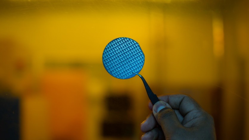
A groundbreaking achievement has been made by scientists from the Indian Institute of Science (IISc), who have introduced a completely homegrown gallium nitride (GaN) power switch that is poised to bring about a transformation in multiple facets of the electronics sector.
The innovative GaN power switch opens up a wealth of possibilities across a wide range of industries, extending from electric mobility to the domain of wireless communications.
As highlighted in a report by Interesting Engineering, this groundbreaking technology was conceived and meticulously developed exclusively within the Center for Nano Science and Engineering (CeNSE) at the Indian Institute of Science (IISc).
For years, Gallium nitride, commonly known as GaN, has garnered acclaim as a high-performance material with immense potential to supplant traditional silicon-based transistors.
In contrast to their silicon counterparts, GaN transistors offer unmatched efficiency and performance, rendering them exceptionally well-suited for applications.
This includes ultrafast chargers, laptops, electric vehicles, and even cutting-edge technologies in the domains of space exploration and military applications like radar systems.
Dr. Digbijoy Nath, an Associate Professor at CeNSE and the lead author of the research study, referred to GaN technology as promising and disruptive. "We don't have gallium nitride wafer production capability at commercial scale in India yet," Dr. Nath stated.
Nevertheless, the constraints on importing GaN materials and devices have presented considerable hurdles for researchers in India. The IISc research team's achievement in creating the power switch is the culmination of extensive years of unwavering dedication to research and innovation.
Emerging from Meticulous Refinement
This groundbreaking technology emerged from the meticulous refinement of a metal-organic chemical vapor deposition technique, which had been honed for over a decade under the guidance of Professor Srinivasan Raghavan, who serves as both a Professor and Chair at CeNSE.
As per the released statement, their approach involves the precise step-by-step cultivation of GaN alloy crystals onto a two-inch silicon wafer, ultimately leading to the creation of a complex, multi-layered transistor.
This intricate procedure demands a carefully controlled environment and the use of a sterile clean room to safeguard against defects caused by fluctuations in humidity and temperature.
Furthermore, the research team collaborated closely with Associate Professor Kaushik Basu and his team from the Department of Electrical Engineering (EE) to construct an electrical circuit utilizing these transistors.
Looking ahead, Science Direct stated that the research team is focused on upscaling the device to handle higher currents and is concurrently working on the development of a versatile power converter capable of voltage transformation.
Dr. Nath highlighted the hurdles faced by strategic organizations in India when it comes to sourcing GaN transistors, emphasizing the limitations on importing them in substantial quantities or with specific power and frequency ratings.
Related Article : US AI Chip Curb Extends to 'Some Middle East' Countries

ⓒ 2026 TECHTIMES.com All rights reserved. Do not reproduce without permission.


