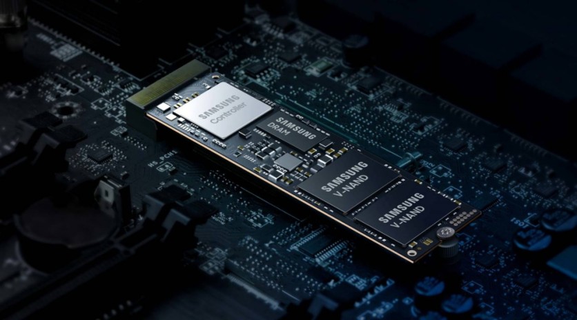
Samsung Electronics has produced the world's first functioning 900-layer V-NAND flash memory prototype — a record that nearly triples the layer count of any chip currently in mass production and signals a fundamental shift in how the semiconductor industry will scale storage for AI servers, data centers, and smartphones. According to Korean semiconductor industry sources on May 25, the company verified normal operation of the memory cells, confirming the 900-layer stack works as a real chip, not merely a theoretical model.
The milestone matters directly to anyone buying or specifying high-density storage: the higher the layer count, the more data fits in a given physical footprint, and the better the power efficiency. At the scale of an AI data center — where thousands of enterprise SSDs operate in parallel — those gains translate into tangible reductions in rack space and power draw. The storage stack inside every AI server, every smartphone, and every cloud SSD traces its density to advances like this one.
The breakthrough was achieved using a technique called Cell Multi-Bonding (CMB), in which Samsung fused two separately manufactured 450-layer cell wafers into a single chip. The approach marks a deliberate departure from the single-stack etching method the company has relied on for more than a decade — a method that reaches physical limits as layer counts climb beyond what a single continuous etch can reliably produce.
Samsung 900-Layer NAND Prototype: How Cell Multi-Bonding Works
Think of conventional 3D NAND as an apartment building constructed floor by floor from a single foundation: all the floors are drilled and stacked in one continuous operation. That works well up to a few hundred floors, but at extreme heights, the structure begins to warp and the drilling loses precision. CMB treats the problem differently. It builds two separate 450-story towers to their maximum reliable height, then precision-bonds them together to form a single 900-story structure.
The engineering obstacles to that bonding step are substantial. As layer counts rise, wafer warpage and stack misalignment become the dominant barriers to yield. Samsung addressed warpage through a redesigned upper chuck — the fixture that holds the wafer flat during processing — and overcame alignment errors with an updated overlay correction technique. The company also refined the bitline and wordline architecture inside the bonded chip, reducing chip size and lowering power consumption in the final device.
The result is a chip whose cell operation characteristics Samsung has verified — meaning the electrical behavior of the memory cells meets expected parameters — even though the prototype is still in the research phase and not ready for mass production.
Read more: Kioxia NAND Flash Mass Production Accelerates: BiCS10 Target Puts Samsung and SK hynix on Edge
Why 3D NAND Flash Memory Layer Count Shapes AI Infrastructure
NAND flash is the memory technology that stores data at rest — the component inside AI servers' SSDs that holds training datasets, model weights, and inference outputs between compute cycles. Unlike DRAM, which processes data rapidly but loses it when powered off, NAND retains data permanently and scales to enormous capacities.
The layer stacking race exists because physical footprint is fixed. A chip can only be so wide before it becomes economically unmanageable to manufacture. Stacking more layers vertically is how chipmakers increase capacity without expanding the die area — the same logic as building a skyscraper instead of a sprawling campus. Each additional tier of layers also allows manufacturers to spread fixed manufacturing costs across more bits, driving down the cost per gigabyte.
For AI infrastructure specifically, high-layer NAND directly addresses two bottlenecks: the need for enterprise SSDs with multi-terabyte capacities in a single drive bay, and the growing demand for storage that consumes less power per terabyte as data center operators face energy constraints. Samsung has described its next-generation bonding NAND as designed for the AI era, projecting that wafer bonding architectures will boost bit density per unit area by 1.6 times compared to conventional designs.
SK Hynix Samsung NAND Competition: Where the Industry Stands
The 900-layer figure lands at a strategically consequential moment in the NAND market. In current mass production, SK Hynix holds the layer-count lead with its 321-layer 4D NAND chips. Samsung's own highest-layer chip in mass production is its 9th-generation V-NAND, the V9, at 286 layers.
Samsung is simultaneously pressing ahead on two fronts. Its 10th-generation V-NAND — known internally as V10, rated at approximately 430 layers — is in the process of ramping toward full-scale mass production, with line construction underway and output targeted for the second half of 2026. The 900-layer CMB prototype, by contrast, is a research-stage achievement — it establishes the technical feasibility of multi-wafer bonding at extreme stack heights, but it will require significant further development before it can be manufactured at commercially viable yields.
Japan's Kioxia, which confirmed its BiCS10 at 332 layers as a fiscal year 2026 production priority just one day before Samsung's announcement, is also developing a comparable multi-stack approach it calls CMOS-directly-Bonded-to-Array. China's Yangtze Memory Technologies is advancing toward 300-layer NAND with strong domestic investment. Micron is developing next-generation NAND with an architecture designed to skip several layer-count nodes in a single step.
The CMB achievement positions Samsung to enter a future generation of NAND — broadly aligned with its stated 1,000-layer target for 2030 — using a technique that its competitors are pursuing independently under different names.
How Does Samsung CMB Compare to Hybrid Bonding From Rivals?
CMB — Cell Multi-Bonding — is Samsung's variant of the broader class of wafer-bonding techniques that the entire NAND industry is converging on as single-stack etching approaches its physical ceiling. The fundamental problem is the same across all manufacturers: drilling the narrow cylindrical holes that form the vertical memory cells through hundreds of layers becomes increasingly unreliable beyond roughly 400 to 500 layers in a single etch, because the drill path deflects and the wafer distorts under accumulated stress.
The industry's responses differ in the details. Kioxia's CMOS-directly-Bonded-to-Array separates the memory cell array from the peripheral control circuits onto different wafers before bonding. China's Yangtze Memory Technologies pioneered its Xtacking architecture — now in its fourth generation — which similarly decouples memory and logic dies. Samsung's CMB bonds two full cell stacks rather than separating cells from peripherals, which allows the company to double the effective layer count without redesigning the peripheral circuitry from scratch.
Samsung first commercialized 3D vertical NAND in 2013, becoming the first company in the industry to stack memory cells vertically rather than spreading them across a flat plane. The 900-layer CMB prototype marks the most significant departure from that original single-stack architecture in more than a decade of V-NAND development.
V-NAND 1,000-Layer Roadmap: What Comes After 900 Layers
The 1,000-layer milestone — widely discussed as the industry's next symbolic threshold — is now within sight of the laboratory even as it remains years away from a production line. Samsung's CTO Song Jae-hyuk has indicated that by using wafer bonding technology, the company can implement more than 1,000 layers in a single NAND device, and has described a "multi-BV" NAND structure involving four bonded wafers as the path toward that goal.
That trajectory — from 286 layers in mass production today, through 430 layers in the V10 production ramp, past the 900-layer CMB prototype, toward 1,000 layers by 2030 — illustrates how quickly the field is moving and how completely the transition from single-stack to multi-wafer bonding architectures is reshaping the manufacturing approach. Kioxia has separately stated plans to mass-produce NAND with more than 1,000 layers by 2031.
The near-term commercial question is not whether 1,000-layer NAND can be built — today's announcement suggests it can — but whether it can be built at the yields and unit economics that make it viable for production. That work remains ahead.
Frequently Asked Questions
What is Cell Multi-Bonding, and how does it differ from conventional 3D NAND stacking?
Cell Multi-Bonding (CMB) is a manufacturing technique in which two separately built NAND cell wafers — each stacked to its maximum reliable height — are precision-bonded together to form a single chip with twice the layer count. Conventional 3D NAND stacks all layers through a single continuous etch process on one wafer; CMB avoids the physical limits of that approach by building the two halves independently and joining them afterward.
How does the Samsung 900-layer prototype compare to what competitors ship today?
The highest-layer NAND currently in commercial mass production is SK Hynix's 321-layer chip. Samsung's own highest-volume product is its 9th-generation V-NAND at 286 layers. The 900-layer CMB prototype nearly triples the current production record, but it is a research-phase chip — it has verified cell operation, but yield and manufacturing costs at commercial scale have not yet been demonstrated.
When will 3D NAND flash memory reach 1,000 layers?
Samsung has set 2030 as its target for 1,000-layer NAND production, contingent on the multi-wafer bonding architecture demonstrated by the 900-layer prototype. Kioxia has a separate timeline targeting 1,000-layer mass production by 2031. Both targets depend on solving yield and cost challenges that have not yet been addressed at full production scale.
What does higher NAND layer count mean for AI servers and data storage?
Higher layer counts allow more data to be stored in the same physical area, reducing cost per gigabyte and improving power efficiency per terabyte. For AI data centers, those improvements translate into higher-capacity enterprise SSDs that consume less energy — directly reducing operating costs for hyperscale cloud operators and AI infrastructure builders.
ⓒ 2026 TECHTIMES.com All rights reserved. Do not reproduce without permission.


