Fritzchens Fritz, popular for the photographer's beautiful chip shots, has now done it again with the PlayStation 5 showing exactly what's under the hood of the massively sought after next-generation console. Fritzens Fritz has been popular for his work with other chips as well.
PS5 first unofficial die shot
Quite unlike Microsoft, who was actually quick to showcase its new Xbox Series S as well as Xbox Series X die shots, Sony has actually never really showed just what is inside the hood of the whole PS5 System on a chip. It has already been a couple of months since the PS5 was initially introduced but customers only now get to see exactly what's on the chip with the codename AMD Flute thanks to VideoCardz.
While the whole world now struggles to get a chance to be able to purchase the scarce PS5 restock online, The Verge writes about what is under Sony's next-generation console when put underneath a microscope. This happened literally when they had shown consumers the 40,000 tiny PlayStation symbols that were reportedly hidden in every single gamepad.
A first quick and dirty die-shot of the PS5 APU (better SWIR image will follow). It looks like some Zen 2 FPU parts are missing. pic.twitter.com/PefXCxc3G1
— Fritzchens Fritz (@FritzchensFritz) February 14, 2021
Photographer Fritzchens Frits
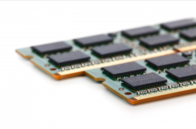
As of the moment and somehow figuratively, consumers have what The Verge believes to be the actual first ever close-up pictures of PS5's actual silicon coming from the photographer Fritzchens Fritz on Twitter. The photos uploaded show Fritz's amazing close-ups of what's seen to be the PlayStation 5's liquid metal interface that is being used by Sony in order to manage the PS5's temperature.
The monochrome portrait pictures of it framed right against the motherboard is interesting to see especially since the photos are shown in high-resolution which most consumers usually won't be able to see with their naked eyes. Fritz then retweeted a tentative die shot analysis which detailed an interpretation of the PS5 floor plan by @Locuza_.
Read Also: Intel i9-11900T 8 Core 35TDP Could Make an Impressive Gaming CPU for Portable Gaming
The interpretation of the PS5 floor plan followed these steps:
1. The Bomba surprise that Sony ahd most likely cut down was from 256-Bit FP pipes all the way to only 128-Bit FP pipes.
2. There was no infinity Cache or L3$. This was also not in the Xbox Series
There could be the old Render Backend design that would need higher resolution in order to say for sure.
4. The said WGPs are all arranged as on RDNA1 GPUs along with two sub-arrays. Just the same as the Xbox Series where the Navi21/22/23, the Rembrandt and Van Gogh only have just one sub-array for all of the WGPs.
5. There is a higher res needed in order to take a closer FPU look as well as the GPU frontend analysis and also certain details like the known Tempest Audio engine.
The article by the verge, however, points out how the PS5's silicon actually stacks up to its known Xbox counterpart or even AMD's own version for PC. However, it was also noted that in the end, results still matter more than the specs itself.
4. The WGPs are arranged as on RDNA1 GPUs with two sub-arrays.
— Locuza (@Locuza_) February 14, 2021
Same goes for the Xbox Series.
Navi21/22/23, Van Gogh and Rembrandt only have one sub-array for all WGPs.
5. Higher res needed for a closer FPU look, GPU frontend analysis and details like the Tempest Audio engine.
Related Article: Nvidia RTX 3060 Release Date February 2021: Is It Better Than RTX 3060 Ti?
This article is owned by Tech Times
Written by Urian Buenconsejo
ⓒ 2026 TECHTIMES.com All rights reserved. Do not reproduce without permission.


