Scientists and material experts have created a new and improved tool called "lab on a chip" that could advance the measurement of light. The team claims that this contributes to the field of spectrometry which could improve everything from environmental monitoring to smartphone cameras.
The project, conducted by Finland's Aalto University, produced a potent, incredibly small spectrometer that fits on a microchip and is run by artificial intelligence. The study was also recently published in Science.
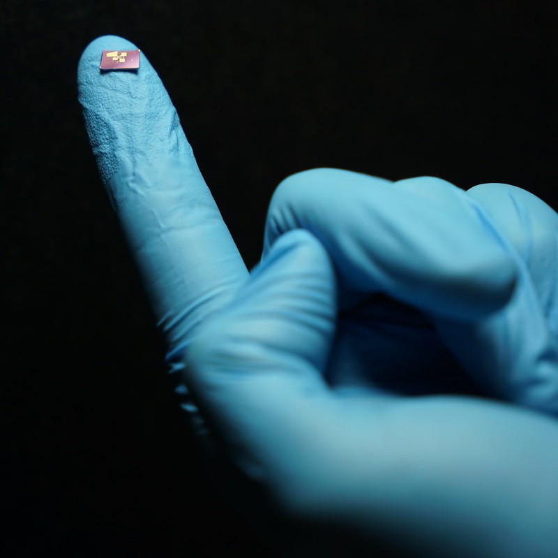
Tiny Spectrometer
Two-dimensional semiconductors are a relatively new class of super-thin materials used in this research. The study's conclusion is a proof-of-concept spectrometer that could be easily incorporated into a variety of technologies, such as security sensors, biomedical analyzers, quality inspection platforms, and space telescopes.
Ethan Minot, a professor of physics at the OSU College of Science, claimed that the new spectrometer could fit on the end of a human hair, in contrast to conventional spectrometers that need large optical and mechanical components.
The new study suggests that those parts might be replaced with innovative semiconductor materials and AI, allowing spectrometers to be drastically scaled down in size from the smallest ones currently available, which are around the size of a grape.
"Our spectrometer does not require assembling separate optical and mechanical components or array designs to disperse and filter light," Hoon Hahn Yoon, the study's lead author, said in a press release statement.
Yoon added that it could reach a high resolution similar to benchtop systems but in a considerably smaller package.
Read also : Intel Eyes Constructing New Semiconductor Mega-Site in Germany; Ireland Fab to Undergo Expansion
100% Electrically Programmable
The device has a huge potential for scalability and wider applicability, according to the researchers, because it is 100% electrically programmable in terms of the hues of light it absorbs.
Yoon claimed that incorporating it directly into portable devices such as smartphones and drones could improve our daily lives. The researcher envisions a future where smartphone cameras could be hyperspectral cameras.
These hyperspectral cameras could pave the way for the imaging and analysis of infrared wavelengths and visible wavelengths.
Minot noted that this would also help environmental monitoring since spectrometers can precisely identify the kind and quantity of pollutants in water, ground, and air.
"If you're into astronomy, you might be interested in measuring the spectrum of light that you collect with your telescope and having that information identify a star or planet. If geology is your hobby, you could identify gemstones by measuring the spectrum of light they absorb," Minot said.
The researcher said that progress in two-dimensional semiconductors could lead to a plethora of discoveries on how their novel optical and electronic properties can be utilized in various settings.
Related Article : 40% of Semiconductor Imports From China Are Defective, Russia Says
This article is owned by Tech Times
Written by Jace Dela Cruz
ⓒ 2026 TECHTIMES.com All rights reserved. Do not reproduce without permission.


